

Megasonic Wafer Cleaning System Brand Comparison for Advanced Semiconductor Manufacturing
2026-11-02
Megasonic cleaning may be the least glamorous step in advanced semiconductor manufacturing, but it remains one of the most unforgiving. As device geometries tighten, a few stubborn particles can collapse yield. This brand comparison cuts through catalog claims to examine real-world performance: transducer uniformity, cavitation control, and process stability. Among the contenders worth a closer look is Siansonic, whose acoustic delivery approach is drawing attention from process engineers tired of settling for 'good enough' particle removal.
Where Megasonic Brands Actually Diverge: Frequency, Power, and Fluid Dynamics
A casual scan of spec sheets might suggest most megasonic cleaning systems look alike, but the moment you map frequency against applied power, real functional gaps appear. One brand might run a fixed 950 kHz transducer while another sweeps between 800 kHz and 1 MHz, and that narrow shift changes how cavitation energy distributes across a wafer surface. Pair that with a power supply that peaks at 20 watts per transducer versus one that holds a true 60 watts under load, and the cleaning behavior stops being a minor variation. It becomes the difference between removing sub-100 nm particles and simply rearranging them.
Fluid dynamics carries equal weight, though it rarely gets headline treatment. The way chemistry flows through a transducer tank, the angle of incidence against the wafer, even the degassing method, all modulate how uniformly energy reaches the surface. Some brands rely on overflow weirs that create dead zones near the edges. Others use bottom-fed laminar flow with carefully placed return ports, keeping the acoustic field more consistent. When you see two machines with the same frequency rating but drastically different particle removal efficiency, the explanation usually sits in these flow-path choices, not in the transducer itself.
The practical takeaway is that matching a megasonic tool to a specific cleaning step requires more than a brand-name comparison. You have to look at how frequency and power interact under real fluid conditions. A tool tuned to 1 MHz with low power might excel at removing particles without damaging fragile structures, but it will struggle with organic residues. Crank up the power and drop to 700 kHz, and you gain removal force while risking pattern collapse. The brands that stand out are the ones that give you control over this balance, not just a single preset that looks good in a demo.
The 950 kHz vs 3 MHz Debate in Damage-Sensitive Device Cleaning
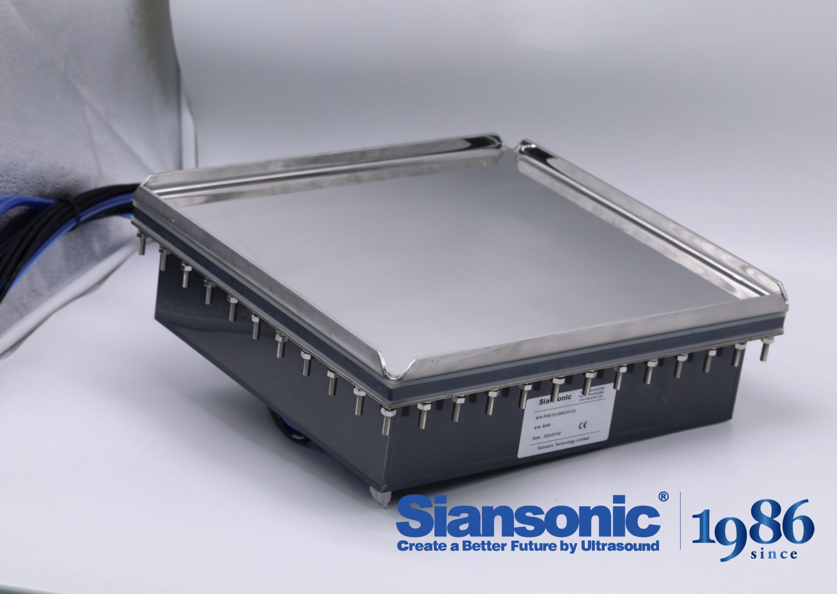
When cleaning damage-sensitive devices such as MEMS accelerometers, surface acoustic wave filters, or advanced photomasks, the choice of ultrasonic frequency often narrows down to two megasonic options: 950 kHz and 3 MHz. Both sit well above conventional ultrasonic cleaning ranges, yet their difference in wavelength and cavitation dynamics creates a persistent divide among process engineers. One camp argues that 950 kHz delivers the mechanical energy needed to dislodge stubborn submicron particles from high-aspect-ratio trenches, while the other insists that 3 MHz offers a gentler touch that preserves fragile cantilevers, thin membranes, and low-k dielectric layers.
The physical basis of this debate lies in how acoustic cavitation scales with frequency. At 950 kHz, the resonant bubble radius is larger, and the cavitation threshold is lower, meaning transient cavitation events occur more readily and with greater intensity. This produces stronger microstreaming and shock waves that can efficiently remove particles even from deep vias or undercut structures, but the same energetic bubble collapses can also erode thin metal lines or crack brittle films. By contrast, 3 MHz operation pushes the cavitation regime toward stable, non-inertial oscillations. Bubbles remain smaller and more numerous, and their collapse energy is distributed over a wider field, reducing peak localized stress. The trade-off becomes obvious: slower particle removal rates, especially for particles below 100 nm, and longer process times that may introduce other risks like galvanic corrosion or chemical residue buildup.
Practitioners rarely settle the debate with a single frequency. Instead, many adopt a sequence or modulation strategy that leverages both regimes. A short initial step at 950 kHz can loosen strongly adhered contaminants, followed by a longer 3 MHz rinse to gently flush away detached particles without inflicting additional damage. Some advanced tools even sweep the frequency continuously between 800 kHz and 3 MHz to avoid standing wave patterns and to tailor cavitation intensity to specific device zones. Ultimately, the optimal choice depends on the exact feature geometry, film stack, and contaminant type—meaning that the 950 kHz vs 3 MHz question is less about which frequency is universally better and more about how precisely one can control the energy delivery to match the device's tolerance.
How Top Suppliers Tune Transducers for Particle Removal Without Pattern Collapse
Top suppliers approach transducer tuning as a dynamic balancing act between acoustic energy delivery and structural protection. Rather than relying on a single fixed frequency, they employ swept-frequency techniques that continuously shift the ultrasonic output across a narrow band. This prevents the formation of standing waves and hot spots where cavitation energy concentrates enough to collapse high-aspect-ratio features. By mapping the resonance modes of the wafer stack—including the device layer, underlying films, and carrier—engineers adjust the driving waveform to match the composite impedance, ensuring that particle removal forces remain uniform across the entire surface.
A key differentiator among leading suppliers is the use of multi-zone transducer arrays. Each zone can be independently tuned in both frequency and power, allowing localized adjustment for varying pattern densities. Dense memory arrays with narrow trenches receive a gentler sweep, while open areas with isolated structures get slightly higher energy for stubborn particle detachment. Real-time feedback from acoustic sensors placed near the wafer surface feeds into the control loop, enabling the system to dial back power the moment it detects the onset of transient cavitation that could damage fragile lines. This closed-loop approach transforms the transducer from a blunt cleaning tool into a precision instrument.
Pulse modulation is another lever that top suppliers pull to avoid pattern collapse. Instead of continuous wave operation, they deliver short, high-intensity bursts followed by quiet intervals that allow the liquid to re-equilibrate. The burst duration and duty cycle are tuned so that particles experience sufficient acceleration to overcome adhesion forces, while the surrounding structures never see sustained stress. Some advanced systems also incorporate harmonic mixing, where a low-frequency fundamental is combined with a higher harmonic to create a tailored pressure field. This lets engineers target specific particle sizes or locations without resorting to excessive overall power—a critical advantage when cleaning wafers with sub-10 nm features.
Cost of Ownership Gaps That Don't Show Up in Vendor Quotes
When comparing hardware or software quotes, the sticker price rarely tells the whole story. Many organizations discover this only after deployment, when line items like data migration labor, integration debugging, and the hours lost to retraining staff start piling up. One manufacturing firm we worked with found that a seemingly cheaper machine vision system ended up costing nearly twice as much as the competitor's after accounting for the custom jigs and the three extra weeks of on-site calibration the vendor hadn't mentioned during the sales cycle.
Hidden costs also hide in the spaces between vendor responsibilities. For example, who absorbs the downtime when firmware updates conflict with existing control software? Who pays for the electricity, cooling, or rack space if the new solution runs hotter than the old one? These gaps often surface as internal friction—IT blames operations, operations blames procurement—rather than as a neat line in a purchase order. A long-term view means mapping every touchpoint from unboxing to decommissioning, and asking vendors pointed questions about what happens when things don't go according to plan.
Perhaps the most overlooked gap is the opportunity cost of a tool that underdelivers in practice. A quote might show identical specs, but if one platform requires twice as many clicks to complete a routine task, that inefficiency compounds daily across every employee. Smart buyers run short pilot programs that measure real user friction, not just benchmark scores. They also build realistic contingency budgets—typically 15 to 25 percent above the quoted price—for the unspoken costs that emerge only after the contract is signed.
Advanced Packaging and High-Aspect-Ratio Cleaning: Who Actually Delivers?
Most equipment vendors talk about high-aspect-ratio cleaning, but only a handful can show consistent particle removal below 0.1 µm in structures deeper than 10:1. The gap between a datasheet and a real wafer map becomes obvious once you look at defect density after multiple rinse and dry cycles.
The suppliers that actually deliver tend to pair custom nozzle design with chemistry tuned for the specific photoresist and etch byproducts. They also control wafer temperature and cavitation energy instead of relying on a standard megasonic bath. Without that level of integration, you get either under-cleaning at the bottom of vias or damage to low-k materials near the top.
When evaluating a vendor, ask for split-lot data from a comparable process flow, not just a demo coupon. The real test is whether their cleaning step holds up after integration with subsequent CMP, plating, or bonding steps. Those who can provide that evidence without a long sales pitch are the ones worth a pilot run.
Service, Recipe Portability, and the Realities of Fab Integration
In semiconductor manufacturing, the promise of recipe portability often collides with the stubborn realities of fab integration. A process recipe that runs flawlessly in one fab can drift, fail, or demand costly re-qualification when transferred to another site. The variance stems from subtle differences in chamber conditioning, gas delivery dynamics, metrology baselines, and even operator habits—none of which are fully captured in a standard recipe file.
Service teams that understand this gap play a decisive role. Instead of treating a recipe as a self-contained artifact, they approach portability as an exercise in context translation. This means auditing the source fab's control limits, mapping sensor offsets, and adjusting for local consumables or maintenance schedules before the first wafer is run. The goal is not to replicate the original recipe exactly, but to reproduce its intended process window under new conditions.
Fab integration, then, is less about moving files and more about negotiating physical and operational differences. Teams that ignore this end up chasing phantom defects or burning engineering hours on unexplained CD shifts. Those that embrace it can shrink ramp times, preserve yield curves, and turn a supposedly smooth transfer into a genuine competitive advantage.
FAQ
ACM Research and Modutek are the most visible in high-volume fabs. ACM Research has gained traction with its SAPS and TEBO technologies aimed at reducing pattern damage while cleaning sub-10nm structures. Modutek focuses on more traditional quartz and stainless steel tanks with adjustable frequency sweeping, often preferred for batch processing of 150mm and 200mm wafers where cost per wafer is critical. SCREEN and Tokyo Electron also offer integrated wet benches with megasonic options, but their systems are usually part of broader process tools rather than standalone cleaners.
ACM Research uses transducer arrays with multiple frequencies and moving megasonic nozzles to create uniform cavitation control, with TEBO specifically addressing bubble implosion damage on fragile patterns. Modutek's systems rely on single or dual fixed transducers at 950kHz or 1MHz mounted on tank bottoms, with frequency sweep to avoid standing waves. The difference shows up in cleaning high-aspect-ratio features: ACM's moving nozzle can direct energy more precisely, while Modutek's tank design is simpler and easier to maintain.
Higher frequencies around 1MHz produce smaller cavitation bubbles and gentler cleaning, which reduces damage to 3D NAND stacks and FinFET gates. Lower frequencies near 40kHz or 80kHz are more aggressive and better for removing larger particles from blanket films or backside cleaning. Brands like ACM Research support dynamic frequency tuning during a single process, whereas many Modutek systems require changing transducer modules to shift frequency, which adds downtime.
Chemical compatibility is often overlooked. Megasonic energy accelerates chemical reactions, so a system's ability to handle SC1, SC2, and dilute HF without degrading seals or transducer bonding matters. For advanced packaging, wafer warpage control becomes critical. Systems with rotating megasonic nozzles, like ACM's, can follow the wafer topography, while fixed-tank designs from Modutek may leave edge zones under-cleaned on warped panels. Also check particle adders after cleaning; some brands have better filtration integration.
Thin wafers demand low mechanical stress and precise fluid dynamics. ACM Research's single-wafer megasonic tools with Bernoulli chuck or edge-grip handling perform better on 50 to 100µm wafers used for TSV and 3D stacking. Modutek's batch tanks, while cost-effective, require cassettes that can induce flexing and non-uniform acoustic fields on ultra-thin substrates. For 300mm thin wafer cleaning, SCREEN's SU-3200 also offers stable megasonic support, but it's typically integrated into a coater/developer track rather than a standalone option.
Modutek systems have lower upfront cost and simpler maintenance because transducers are user-replaceable and tanks are built from quartz or PVDF. ACM Research's single-wafer platforms cost more initially but reduce chemical usage by up to 30% through recirculation and precise dispense, which matters for high-volume fabs running 20,000 wafers per month. Tokyo Electron's wet benches often carry a premium due to integration with factory automation, but their service contracts are more globally standardized. Batch systems can process 25 to 50 wafers at once, but a single failed transducer can idle the entire tank.
Yes, and it's a growing differentiator. SiC wafers are harder and chemically inert, requiring higher acoustic power density to dislodge particles from polished surfaces. ACM Research has demonstrated process recipes for 150mm and 200mm SiC using dual-frequency megasonic nozzles combined with heated SC1. Modutek offers higher wattage transducers, up to 600W per tank, that can be tuned for SiC batches, but the lack of moving nozzle limits uniformity across 200mm substrates. For GaN-on-Si, lower megasonic power is preferred to avoid damaging the epi layer, which favors systems with real-time power monitoring like those from MEI Wet Processing.
Service response can outweigh technical specs. ACM Research has expanded rapidly but still has thinner field service coverage in Europe compared to SCREEN or Tokyo Electron. Modutek is a smaller specialist with direct factory support and quick customization, which suits fabs needing rapid tank modifications. For advanced semiconductor manufacturing, where unscheduled downtime costs over $100k per hour, choosing a brand with local spare parts inventory and trained engineers within a four-hour radius is often more critical than a 2% difference in particle removal.
Conclusion
Comparing megasonic wafer cleaning systems across major brands for advanced semiconductor manufacturing quickly moves past brochure specifications into territory where real differences emerge: how each vendor manages frequency, power delivery, and fluid dynamics inside the process tank. A central tension remains between 950 kHz and 3 MHz operation. The lower frequency generates more aggressive cavitation energy that strips stubborn particles efficiently, yet it raises the risk of pattern collapse on densely packed, damage-sensitive structures. The higher frequency produces a milder, more uniform acoustic field with smaller transient bubbles, making it preferable for fragile gate stacks or narrow-pitch interconnects, but it often demands longer process times or higher power to match cleaning performance. Top suppliers have responded in different ways: some use segmented transducer arrays that sweep frequency across a narrow band to avoid standing waves, others modulate power in pulsed sequences to control cavitation intensity near wafer edges, and a few integrate nozzle-based or laminar flow designs that keep particles in suspension rather than redepositing them. These choices directly affect not only particle removal efficiency but also the survival rate of high-aspect-ratio features after cleaning.
Beyond the physics, brand comparison reveals that cost of ownership gaps rarely appear on vendor quotes. Consumables such as specialized chemistry filters, transducer replacement intervals, and energy consumption under real fab duty cycles can shift the long-term economics significantly. Advanced packaging and high-aspect-ratio cleaning separate suppliers further: some have proven, repeatable recipes for through-silicon vias, microbumps, and deep trench structures, while others only claim capability without demonstrating yield data on actual product wafers. Service models, recipe portability, and fab integration add another layer. A tool that excels in a lab demo may struggle when recipes need to transfer across multiple sites or when local support is thin. The most competitive brands pair robust transducer engineering with transparent ownership data and a track record of adapting to new device architectures without forcing customers into rigid, hard-to-port cleaning sequences.
Contact Us
Contact Person: Ivy Zhang
Email: [email protected]
Tel/WhatsApp: +86 1081502288
Website: https://www.siansonic.com/